

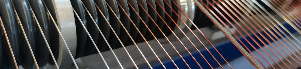
PV busbars (also known as solder ribbons) are core metallic conductive materials in photovoltaic (PV) modules, responsible for interconnecting solar cells and conducting current. Copper foil serves as the predominant substrate material for PV busbars, fulfilling critical functions including current collection between solar cells, low-resistance electrical conduction, mechanical interconnection, and long-term reliability. With the evolution of crystalline silicon (c-Si) cell technology—from BSF/PERC to N-type technologies such as TOPCon, HJT, and IBC—and the rapid advancement of multi-busbar (MBB) and zero-busbar (0BB) architectures, PV busbars impose increasingly stringent requirements on copper foil regarding dimensional specifications, surface treatment, solderability, mechanical strength, and PID (potential-induced degradation) resistance. This document systematically addresses the fundamental structure of PV modules, types and functions of busbars, the critical role of copper foil in PV busbars, comparative analysis of copper versus aluminum foil, classifications and specifications of copper foil, manufacturing processes, typical applications, key performance requirements, selection criteria, and future development trends.
Basic Structure and Working Principle of PV Modules
Photovoltaic (PV) modules—also known as solar panels—are the core power-generating units of photovoltaic power generation systems. They consist of multiple solar cells interconnected in series and/or parallel via busbars/ribbons to directly convert light energy into electrical energy. The basic structural configuration of a PV module, from front to back, comprises: tempered glass front cover, front encapsulant film (EVA—ethylene-vinyl acetate copolymer), solar cells, interconnector ribbons, rear encapsulant film (EVA), backsheet—or dual-glass front cover—and aluminum frame, junction box, and connector.
Regarding solar cells, the mainstream photovoltaic (PV) cells are crystalline silicon solar cells. Cell dimensions have progressively increased—from M2 (156.75 mm), M4 (161.75 mm), M6 (166 mm), M10 (182 mm) to M12 (210 mm)—with M10 and M12 currently dominating the market. Cell thickness has been reduced from 180 μm to 130–150 μm. PV cell technology pathways include:
- Aluminum Back Surface Field (BSF): First-generation crystalline silicon solar cells, with efficiency of 17–19%, now largely obsolete
- Passivated Emitter and Rear Cell (PERC): Second-generation mainstream solar cells, with efficiency of 22–23%
- Passivated Emitter Rear Totally diffused (PERT): Bifacial power-generating solar cells
- Heterojunction (HJT): N-type amorphous silicon/crystalline silicon heterojunction, with efficiency of 24–26%
- Tunnel Oxide Passivated Contact (TOPCon): Tunnel oxide passivated contact technology, with efficiency of 24–26%
- Interdigitated Back Contact (IBC): Back-contact solar cells, with efficiency of 25–27%
- Perovskite/Silicon Tandem: Lab-scale efficiency >33%, under mass production
Thin-film solar cells—including CIGS (copper indium gallium selenide), CdTe (cadmium telluride), and CZTSSe (copper zinc tin sulfur selenide)—exhibit superior low-light performance and flexibility/bendability, but their efficiency is 18–22% lower than that of crystalline silicon.
Regarding the operating principle of photovoltaic (PV) modules, the photovoltaic effect enables solar cells to generate photocurrent under illumination. A single cell produces an output voltage of approximately 0.5–0.65 V and an output power of approximately 5–7 W (PERC M10). To achieve the module’s operating voltage (typically 30–50 V DC) and power rating (300–700 W), 60 or 72 cells are interconnected in series/parallel configurations to form a string. Electrical interconnection between cells is accomplished via busbars.
Regarding the main busbar of solar cells, the main busbar (Main Busbar/Finger) refers to the fine metal grid electrodes on the front side of the solar cell, designed to collect photogenerated current and conduct it to the tabbing ribbon. Early solar cells employed a 2-busbar (2BB) design; currently, multi-busbar (MBB) designs with 5BB, 9BB, 12BB, 16BB, and 20BB configurations have been developed. MBB technology reduces the lateral current transmission distance within the solar cell, significantly lowering series resistance and improving cell efficiency by 0.5–1%.
In photovoltaic (PV) module electrical interconnections, solar cells are series-welded using interconnector ribbons (also known as tabbing ribbons) to form cell strings. Multiple cell strings are then paralleled inside the junction box via string ribbons and bypass diodes, with output routed to the junction box terminals and connected externally—via MC4 or other compatible connectors—to inverters, combiner boxes, and the grid.
Regarding electrical parameters of photovoltaic (PV) modules, mainstream PV modules feature the following electrical specifications: peak power output of 300–700 W (monocrystalline silicon—M10 60-cell: 360–400 W; M10 72-cell: 430–460 W; M12 60-cell: 480–550 W; M12 72-cell: 550–700 W); open-circuit voltage (Voc): 40–50 V; maximum power point voltage (Vmp): 33–42 V; short-circuit current (Isc): 10–18 A; maximum power point current (Imp): 9–16 A; maximum system voltage: 1500 V DC; module efficiency: 19–22 %.
Types and Functions of PV Busbar Ribbon
PV busbars/ribbons are metallic conductive interconnection strips between solar cells and between solar cell strings and junction boxes, constituting one of the key materials in photovoltaic modules. Busbars/ribbons are classified according to position, function, geometry, and plating.
Classified by location and function, busbars mainly include:
- Main grid interconnection tabbing ribbon/stringer ribbon: A flat metal ribbon connecting the positive and negative terminals of adjacent solar cells, with a width of 1.0–1.6 mm and thickness of 0.15–0.30 mm; at least two ribbons are welded on each side (front and back) of every cell.
- Busbar/collecting ribbon: A metal ribbon connecting cell strings to junction box terminals, with a width of 4–8 mm and thickness of 0.20–0.40 mm, designed to carry higher current.
- Round ribbon: A round-section ribbon with a diameter of 0.8–1.5 mm, used in specific cell manufacturing processes.
- Shaped ribbon: A ribbon with non-circular cross-sections—e.g., D-shaped, elliptical, or triangular—to enhance optical reflectivity (light utilization efficiency).
- Black ribbon: A ribbon coated with a black layer (black nickel + black tin) to reduce reflectivity and improve module aesthetics.
- Zero-main-grid (0BB) ribbon: A conductive adhesive or adhesive film used in 0BB technology, replacing conventional metallic tabbing ribbons.
Classified by manufacturing process and coating, busbars are primarily divided into:
- Plain Copper Ribbon: Bare copper ribbon requiring surface treatment
- Tin-coated Copper Ribbon (TC Ribbon): Copper ribbon with an electrodeposited tin coating (Sn 5–25 μm); the most widely adopted solution
- Tin-Lead coated Copper Ribbon (TLC Ribbon): Copper ribbon with an electrodeposited tin-lead alloy coating (SnPb 5–25 μm); a conventional solution
- Nickel-coated Copper Ribbon: Copper ribbon with an electrodeposited nickel coating (Ni 1–5 μm); resistant to potential-induced degradation (PID) and corrosion
- Silver-coated Copper Ribbon: Copper ribbon with an electrodeposited silver coating (Ag 1–3 μm); highest electrical conductivity
- Low-silver/Non-silver coated ribbons: Reduced silver content or alternative coatings such as SnBi/SnAg
- Tin-coated Copper Clad Aluminum Ribbon (CCA Ribbon): Composite material consisting of an aluminum core clad with copper
Core functional aspects of busbars:
- Current collection and transmission: guiding the photogenerated current from solar cells through main busbar electrodes to the junction box
- Low-resistance connection: minimizing power loss and enhancing module efficiency via low-resistance interconnections
- Mechanical interconnection: achieving both mechanical fixation and electrical connection between solar cells through soldering
- Stress buffering: absorbing stresses induced by solar cell thermal expansion, vibration, and wind/snow loads
- Long-term reliability: ensuring electrical connection reliability throughout the module’s 25-year service life
Key parameters of busbars in photovoltaic modules: width 1.0–2.0 mm (interconnect ribbons), 4–8 mm (busbars); thickness 0.15–0.40 mm; length customized according to cell dimensions (interconnect ribbon length for M10/M12 cells approx. 165–210 mm); resistivity <2.2×10⁻⁸ Ω·m (pure copper); solder joint strength ≥1.0 N/mm; tensile strength ≥150 MPa; elongation ≥20%.
Key Functions of Copper Foil in PV Busbar
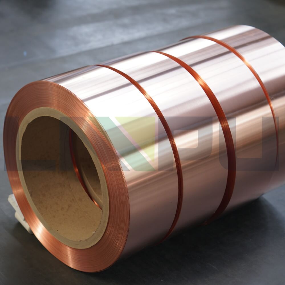
Copper foil serves multiple critical functions in photovoltaic busbars: low-resistance conduction, solder interconnection, mechanical support, thermal expansion matching, and corrosion protection.
Regarding low-resistance conductivity, copper exhibits 100% IACS (International Annealed Copper Standard) conductivity and a resistivity of 1.724×10⁻⁸ Ω·m at 20°C, making it the second-most conductive metallic material after silver (106% IACS). Photovoltaic (PV) busbars must carry the operating current of solar cells (individual cell Imp: 9–16 A; full string: up to 10–15 A); using pure copper foil as the substrate significantly reduces resistive losses. The low resistance of copper foil improves module efficiency by 0.2–0.5% and increases cumulative energy generation over 25 years by 5–10%.
Regarding welding interconnections, photovoltaic busbars are connected to solar cell electrodes via welding processes. Welding methods include infrared soldering (IR), hot air soldering (HAS), electromagnetic induction soldering, and laser soldering. Welding temperature: 200–380 °C; welding time: 1–5 seconds. The tin plating layer (Sn, 5–25 μm) on the copper foil surface melts at the welding temperature (Sn melting point: 232 °C), forming Cu–Sn intermetallic compounds (IMCs, e.g., Cu₆Sn₅, Cu₃Sn) to achieve metallurgical bonding. Weld strength reaches 1.0–3.0 N/mm, satisfying the IEC 61215 tensile test requirements.
Regarding mechanical support, photovoltaic modules deployed outdoors must withstand wind loads (2400–5400 Pa), snow loads (5400 Pa), hail impact (25 mm hailstones at 23 m/s), thermal cycling (–40 °C to +85 °C, 200 cycles), damp heat cycling (85 °C/85 % RH, 1000 h), and mechanical vibration. The high tensile strength (220–300 MPa in O-temper), high elongation (>30 %), and excellent toughness of copper foil prevent cracking and delamination under thermal cycling and mechanical loading.
Regarding thermal expansion matching, the coefficient of thermal expansion (CTE) of silicon solar cells is approximately 2.6×10⁻⁶ /°C, that of copper is approximately 16.5×10⁻⁶ /°C, and that of aluminum is approximately 23.1×10⁻⁶ /°C. The CTE mismatch between copper and silicon (approximately 6.3-fold difference) remains smaller than that between aluminum and silicon (approximately 8.9-fold difference). Under temperature cycling from –40°C to +85°C, the relative deformation between copper foil and solar cells is minimized, thereby preventing solder joint cracking and delamination between copper foil and solar cells caused by thermal stress. This is one of the key reasons why copper foil outperforms aluminum foil in photovoltaic (PV) busbar applications.
Regarding corrosion protection, copper readily oxidizes in ambient air to form copper oxide (CuO, Cu₂O); the resulting oxide layer is non-conductive and adversely affects solderability. Surface treatments such as tin (Sn), nickel (Ni), or silver (Ag) plating are applied to copper foil to form a protective layer, thereby enhancing oxidation resistance and corrosion resistance. Over the 25-year service life of photovoltaic modules, the plated coating on copper foil is critical to ensuring long-term reliability.
Regarding battery efficiency, the width of the busbar directly affects the shading area on the solar cell. In early 2BB technology, the busbar width was 1.5–2.0 mm, resulting in a shading area accounting for approximately 3–4% of the solar cell area. MBB technology reduces the busbar width to 1.0–1.5 mm, decreasing shading per individual busbar by 30–50%; however, the number of main grid lines increases 5–10-fold, reducing the total shading area to 1.5–2.5% and increasing module power output by 1–2%. Circular or shaped busbars, incorporating optical reflection design, enable secondary reflection of incident light onto the solar cell, further minimizing optical losses.
Comparison of Copper Foil and Aluminum Foil
Copper foil and aluminum foil are the two primary substrate materials for PV busbars, exhibiting significant differences in electrical conductivity, weight, cost, solderability, mechanical properties, and weather resistance.
Regarding conductivity, copper has a conductivity of 100% IACS, while aluminum has a conductivity of approximately 61% IACS. At the same cross-sectional area, the resistance of copper foil is about 60% that of aluminum foil. The resistance of photovoltaic busbars directly determines the module’s series resistance (Rs); an increase of 0.1 Ω in Rs can reduce module power output by 0.5–1 W. In applications involving large-format cells (M10/M12) and high-efficiency cells (TOPCon/HJT), the low-resistance advantage of copper foil is critical to module efficiency.
Regarding weight, the density of copper is 8.96 g/cm³ and that of aluminum is 2.70 g/cm³; thus, copper weighs approximately 3.3 times as much as aluminum. In photovoltaic modules, the total weight of copper foil busbars is approximately 0.3–0.8 kg per module (60–72-cell modules), accounting for 3–5% of the module’s total weight. Replacing copper foil with aluminum foil reduces weight by 50–70%; however, the cross-sectional area of the aluminum foil must be increased (to approximately 1.6 times that of the copper foil) to maintain equivalent resistance, thereby reducing the weight advantage to 30–40%.
From a cost perspective, the market price of copper is approximately three to four times that of aluminum (based on 2024 data: copper at approximately CNY 60–80/kg, aluminum at approximately CNY 18–25/kg; PV ribbon FOB USD 20.28/kg). Copper foil incurs significantly higher costs compared to aluminum foil. In mass production of large-scale photovoltaic modules (550–700 W), busbar cost accounts for approximately 5–8% of the module’s balance-of-system material cost. In high-efficiency modules employing HJT/TOPCon cells—where efficiency sensitivity is critical—the low-resistance advantage of copper foil outweighs its incremental cost.
Regarding solderability, tinned, tin-lead plated, nickel-plated, or silver-plated copper foil exhibits excellent solderability at soldering temperatures of 200–380 °C, enabling reliable Cu–Sn intermetallic compound bonding with solar cell electrodes (silver paste, silver–aluminum paste, or copper paste). The dense and stable native aluminum oxide layer (Al₂O₃) on aluminum foil impedes soldering; therefore, specialized processes—such as ultrasonic-assisted soldering, low-temperature brazing, or conductive adhesives—or surface treatments—such as nickel plating or copper plating—are required to achieve solderability. Copper foil demonstrates significantly higher soldering maturity and reliability compared to aluminum foil.
Regarding mechanical properties, the tensile strength of copper is 220–400 MPa, with elongation of 15–30%; that of aluminum is 80–150 MPa (O-temper), with elongation of 20–35%. Copper foil exhibits significantly higher strength than aluminum foil, though its elongation (ductility) is slightly lower. Under photovoltaic module temperature cycling (−40 °C to +85 °C) and mechanical loading, the superior strength of copper foil renders it less prone to fracture and delamination.
Regarding thermal expansion, the CTE of copper is approximately 16.5×10⁻⁶ /°C, that of aluminum is approximately 23.1×10⁻⁶ /°C, and that of silicon is approximately 2.6×10⁻⁶ /°C. The CTE mismatch between copper and silicon is smaller than that between aluminum and silicon; thus, copper foil exhibits superior thermal stress matching with silicon wafers compared to aluminum foil. Copper foil presents a lower risk of solder joint cracking under thermal cycling conditions.
Regarding weather resistance, copper is prone to oxidation and discoloration in atmospheric conditions; however, its weather resistance is significantly improved when plated with tin, nickel, or silver. Aluminum forms a dense Al₂O₃ oxide layer in atmospheric environments, providing excellent weather resistance. Copper foil busbars may develop patina (basic copper carbonate) over a 25-year service life, potentially impairing conductivity; therefore, stringent coating protection is required. Aluminum foil exhibits superior atmospheric weather resistance; however, the weather resistance of aluminum foil weld joints is inferior to that of copper foil weld joints.
Regarding current applications, copper foil busbars remain the dominant solution in the photovoltaic (PV) module busbar market (>95% market share), while aluminum foil busbars are applied only in a few low-end modules and zero-busbar (0BB) technologies. The low-temperature soldering process (<200°C) used in heterojunction (HJT) cells increases the feasibility of aluminum foil and copper-clad aluminum (CCA) busbars; however, copper foil busbars still prevail.
Types and Specifications of Copper Foil
Copper foil for PV busbars is classified according to manufacturing process, alloy composition, temper, thickness, and surface treatment.
In terms of manufacturing process, copper foil is categorized into two major types:
- Rolled Annealed (RA) Copper Foil: Manufactured via a rolling process, wherein electrolytic copper plates or copper ingots undergo multiple cycles of cold rolling and annealing to produce copper foil. Characteristics of RA copper foil include smooth surfaces on both sides, excellent flexibility, and high elongation (>30%). Typical thickness: 0.10–0.50 mm. RA copper foil is the predominant substrate material for PV busbars.
- Electrodeposited (ED) Copper Foil: Manufactured via an electrodeposition process. Characteristics of ED copper foil include one smooth side and one rough side, with surface roughness (Ra) ranging from 0.5–5 μm. Typical thickness: 0.035–0.210 mm (1–6 oz). ED copper foil sees limited application in PV busbars and is primarily used in PCBs.
Regarding alloy composition, PV busbar copper foil is primarily made of electrolytic tough pitch copper (e.g., C1100, C1220), with a minimum purity of 99.95%. For certain specialized applications, oxygen-free copper (OFC) is used to enhance solderability and corrosion resistance.
Regarding temper, copper foil is classified into hard (H), half-hard (1/2H), and annealed (O) based on the degree of annealing. PV busbar copper foil primarily employs annealed (O) or half-hard (1/2H) rolled copper foil to ensure bending performance and soldering strength. Hard-temper copper foil exhibits low elongation (<10%) and is prone to cracking during bending; therefore, it is unsuitable for PV busbars.
Regarding thickness, common thickness specifications for PV busbar copper foil:
- 0.10–0.15 mm: MBB (Multi-Busbar) interconnection ribbon, thin-gauge, low-light-shielding
- 0.18–0.25 mm: Standard interconnection ribbon, mainstream gauge
- 0.25–0.30 mm: Interconnection ribbon for double-glass/large-format modules
- 0.30–0.40 mm: Busbar ribbon (for connecting cell strings to junction boxes), high-current applications
In terms of width, common width specifications for PV busbar copper foil:
- 1.0–1.2 mm: Round or shaped busbars
- 1.4–1.6 mm: MBB (Multi-Busbar) interconnection ribbons
- 1.8–2.0 mm: Conventional interconnection ribbons
- 4–6 mm: Busbars
- 6–8 mm: High-current busbars
- 10 mm: Special high-power module busbars
Regarding surface treatment, the surface treatment of copper foil is a critical process for PV busbars, directly affecting solderability, corrosion resistance, and PID resistance.
- Tin Plating: Surface tin plating layer (Sn, 5–25 μm); the most widely adopted solution. The tin layer is uniform and dense, offering excellent solderability and low cost.
- Tin-Lead Plating: Surface tin-lead alloy plating layer (SnPb, 5–25 μm); a conventional solution. Eutectic SnPb (Sn63Pb37) has a melting point of 183 °C, enabling low-temperature soldering.
- Nickel Plating: Surface nickel plating layer (Ni, 1–5 μm); delivers outstanding PID resistance, used in TOPCon solar cells. The nickel layer enhances corrosion resistance and PID resistance.
- Silver Plating: Surface silver plating layer (Ag, 1–3 μm); provides the highest electrical conductivity and solderability, used in HJT/IBC solar cells.
- Tin-Bismuth Plating: Lead-free plating, environmentally compliant.
- Tin-Silver Plating: Lead-free, high-reliability plating.
- Black Ni + Black Sn: Specialized plating for black busbars, reducing reflectivity.
- Low-Silver/Zero-Silver Plating: Low-silver or zero-silver busbars, reducing silver material costs.
Regarding composite configurations, PV busbar copper foils are available in the following composite forms:
- Plain Copper Foil: Bare copper strip requiring surface treatment
- Tin-Coated Copper Foil: Most widely adopted solution
- Nickel-Coated Copper Foil: Used in PID-resistant applications
- Copper-Clad Aluminum (CCA) Foil: Composite of aluminum core and copper cladding, balancing cost and conductivity
- Tin-Coated CCA Foil: CCA foil with tin coating, mainstream low-cost solution
- Cu-Ni Composite Foil: High PID resistance
- Ag Alloy Composite Foil: Dedicated to HJT solar ce
Manufacturing Process of Copper Foil
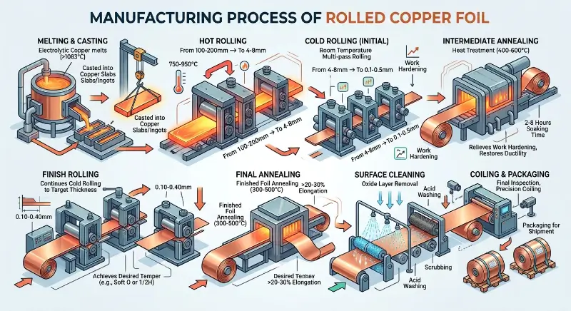
The manufacturing process for copper foil used in PV busbars varies depending on the type. Rolled annealed (RA) copper foil is the predominant substrate material for PV busbars, and its manufacturing process is as follows:
Manufacturing process of rolled annealed copper foil:
- Melting and casting: Electrolytic copper is heated above 1083°C in a melting furnace to melt, then cast into copper slabs or ingots.
- Hot rolling: Copper ingots undergo multi-pass hot rolling on a hot rolling mill, reducing thickness from 100–200 mm to 4–8 mm at a hot rolling temperature of 750–950°C.
- Cold rolling: The hot-rolled copper strip is subjected to multi-pass cold rolling at room temperature, reducing thickness from 4–8 mm to 0.1–0.5 mm; cold rolling induces work hardening.
- Intermediate annealing: Intermediate annealing (400–600°C, held for 2–8 hours) is performed during cold rolling to eliminate work hardening and restore ductility.
- Final cold rolling: Further cold rolling to the target thickness of 0.10–0.40 mm.
- Final annealing: Final annealing (300–500°C) renders the copper foil in soft (O) or half-hard (1/2H) temper, with elongation >20–30%.
- Surface cleaning: Acid pickling and polishing to remove oxide layers.
- Coiling and packaging.
Copper foil surface treatment (electroplating) process:
- Pretreatment: Acid pickling to remove oxide layer, rinsing, activation.
- Electroplating: Electroplating is performed in plating baths according to coating type:
– Tin plating: Stannous sulfate electrolyte, current density 1–5 A/dm², bath temperature 20–40 °C
– Nickel plating: Nickel sulfate + nickel chloride electrolyte, pH 3.5–4.5, current density 2–10 A/dm²
– Silver plating: Cyanide-based or cyanide-free silver electrolyte, current density 0.5–2 A/dm²
– Tin–lead plating: Tin–lead alloy electrolyte, eutectic Sn63Pb37 - Post-treatment: Rinsing, passivation (tarnish prevention), drying.
- Reeling and slitting.
Busbar forming process:
- Slitting: Copper foil strips are slit to specified widths (1.0–8 mm).
- Straightening: Strips are straightened using a straightening machine to eliminate bending and warping.
- Cutting: Strips are cut to cell dimensions to form interconnect ribbons (length: 165–210 mm).
- Chamfering: Both ends of the interconnect ribbons are chamfered to facilitate welding alignment.
- Rewinding and packaging.
Key quality indicators for copper foil:
- Purity: ≥99.95% (C1100, C1220)
- Conductivity: ≥100% IACS
- Thickness tolerance: ±5% to ±10%
- Width tolerance: ±0.05 mm
- Surface roughness: Ra < 0.5 μm
- Tensile strength: O temper 220–300 MPa
- Elongation: O temper >30%
- Hardness: HV 40–60
- Coating thickness: Sn 5–25 μm, Ni 1–5 μm, Ag 1–3 μm
- Coating uniformity: thickness variation ±15%
- Solderability strength: ≥1.0 N/mm
Applications in Crystalline Silicon Solar Cells
Crystalline silicon (c-Si) solar cells are the mainstream cell type for photovoltaic modules, including PERC, TOPCon, HJT, and IBC. The application of copper foil busbars in c-Si solar cells varies depending on the cell technology.
Regarding PERC cells, PERC (Passivated Emitter and Rear Cell) was the mainstream cell technology from 2018 to 2024, with efficiencies of 22–23%. The front-side electrode of PERC cells consists of silver paste fine-line grid (busbars + fingers), while the rear side features an aluminum back surface field (Al-BSF). Tin-plated copper ribbons (Sn: 5–15 μm) are used for interconnection and current collection in PERC cells, with soldering temperatures of 280–340 °C and soldering durations of 1.5–3 seconds. The mainstream specifications for PERC cell current-collecting ribbons are: width 1.0–1.6 mm, thickness 0.18–0.25 mm.
Regarding TOPCon cells, TOPCon (Tunnel Oxide Passivated Contact) is a next-generation cell technology that experienced explosive growth starting in 2024, with efficiencies of 24–26%. The front-side electrode of TOPCon cells consists of fine-line silver–aluminum paste, while the rear side employs poly-Si passivated contacts. A key challenge for TOPCon cells is PID (Potential Induced Degradation): under high system voltage (1500 V), charge accumulation on the cell surface leads to power degradation. TOPCon cell interconnect ribbons typically utilize nickel-plated copper ribbon (Ni 1–3 μm) or nickel + tin composite-plated ribbon, offering excellent PID resistance. Soldering temperature is 280–360 °C, with soldering time of 1–3 seconds.
Regarding HJT cells: HJT (Heterojunction) refers to N-type amorphous silicon/crystalline silicon heterojunction solar cells, with efficiencies of 24–26%. Both the front and rear surfaces of HJT cells feature TCO (Transparent Conductive Oxide) thin films (ITO) plus silver grid-line electrodes. Key challenges for HJT cells:
- Low-temperature process: HJT process temperature < 200 °C (to prevent crystallization of amorphous silicon)
- Soldering temperature limitation: Soldering temperature for HJT cells must be < 200 °C (to avoid TCO damage); low-temperature solder (e.g., SnBi, SnIn, melting point 100–180 °C) is required
- Silver-containing paste: HJT cells employ low-temperature silver paste with high silver content
The busbars for HJT cells typically employ tinned copper strips (low-melting-point coating), nickel-plated copper strips, silver-plated copper strips (high conductivity), and lead-free low-temperature solder. The MBB technology for HJT cells (9BB/12BB/16BB/20BB) is the most widely adopted, utilizing round busbars or shaped busbars with diameters of 0.6–1.0 mm.
Regarding IBC (Interdigitated Back Contact) cells: IBC is a back-contact solar cell with an efficiency of 25–27%. Both the positive and negative electrodes of the IBC cell are located on the rear side of the cell, and the front side features no main busbars. Flat copper foil current-collecting straps are used to directly connect the positive and negative electrode pads on the rear side of the IBC cell; the copper foil has a width of 1.0–1.5 mm and a thickness of 0.15–0.25 mm. The current-collecting strap welding technology for IBC cells is complex, requiring precise alignment and low-temperature welding.
Regarding MBB (Multi-Busbar) technology, the number of main busbars on solar cells is increased from 2BB/5BB to 9BB/12BB/16BB/20BB. Specifications of copper foil current-collecting strips for MBB technology:
- Round ribbon: diameter 0.4–0.8 mm; circular cross-section facilitates reduced light shielding and optical reflectance
- Shaped ribbon: D-shaped, elliptical, or triangular profile; enhances optical reflectance
- Flat ribbon: width 1.0–1.5 mm, thickness 0.15–0.20 mm
Advantages of MBB technology: reduction of internal series resistance of solar cells by 5–10%, improvement of module efficiency by 0.5–1%, reduction of silver paste consumption by 30–50%, and enhancement of module reliability.
Regarding 0BB (Zero Busbar) technology, 0BB represents the next-generation busbar-free technology, eliminating the front-side main busbars on solar cells and achieving electrical interconnection via conductive adhesives, adhesive films, copper wires, or copper foils. Application of copper foil in 0BB technology:
- SmartWire (Meyer Burger): Tin-plated copper wire with diameter 0.1–0.2 mm, fixed to the front side of solar cells using an adhesive film (EVA substitute)
- Copper foil adhesive film: Ultra-thin copper foil (thickness 0.05–0.10 mm) replacing the main busbar
- Copper foil conductive adhesive: Electrical interconnection achieved using copper foil combined with conductive adhesive
Advantages of 0BB technology: component efficiency improvement of 0.5–1%, silver paste consumption reduction of 70–100%, and cost reduction of 5–10%. 0BB technology is a key technical focus area for 2024–2025.
Regarding perovskite/silicon tandem cells, perovskite/silicon tandem cells represent the next-generation high-efficiency photovoltaic cells, with laboratory efficiencies exceeding 33%. In tandem cells, the top cell is perovskite-based, while the bottom cell is crystalline silicon-based (TOPCon/HJT). The copper foil current-collecting tabs for tandem cells require low-temperature soldering (<150°C), fine pitch (0.6–1.0 mm width), and high conductivity (low resistive losses).
Applications in Thin-Film Solar Cells
Thin-film solar cells—including CIGS (copper indium gallium selenide), CdTe (cadmium telluride), and CZTSSe (copper zinc tin sulfur selenide)—offer advantages such as superior low-light performance, flexibility, and low temperature coefficients. The application of copper foil busbars in thin-film solar cells differs from that in crystalline silicon solar cells.
Regarding CIGS (Copper Indium Gallium Selenide) solar cells, their efficiency ranges from 18% to 22%, offering advantages such as excellent low-light performance, low temperature coefficient, and flexibility. The electrode structure of CIGS solar cells is as follows: the front side comprises ZnO/CdS/CIGS/Cu(In,Ga)Se₂/Mo/stainless steel or soda-lime glass, while the back side features a Mo back electrode. Interconnection of CIGS cells employs copper foil busbars with either Sn or Ag plating, having a width of 1.5–2.0 mm and thickness of 0.20–0.30 mm. Flexible CIGS solar cells utilize thinner copper foil (0.10–0.15 mm) and flexible substrates (e.g., stainless steel or polyimide [PI]).
Regarding CdTe (Cadmium Telluride) solar cells, their efficiency ranges from 18% to 20%, with First Solar as the representative manufacturer. The electrode structure of CdTe solar cells is: front side—TCO/CdS/CdTe/back electrode. Interconnection of CdTe cells employs copper foil busbars with lead-free SnBi plating, and soldering temperature is <200°C. CdTe modules are predominantly large-format (1.6 m × 1.2 m) and double-glass structured, featuring larger-dimension busbars.
Characteristics of copper foil applications in thin-film batteries:
– Thinner thickness: 0.10–0.20 mm (for flexible applications)
– Surface treatment: Low-temperature solder (SnBi, SnIn), lead-free and environmentally compliant
– Higher precision: Width tolerance ±0.02 mm (for fine interconnection)
– Flexibility: Bendable and curlable
Although thin-film solar cells hold a smaller market share than crystalline silicon solar cells (<5%), they offer distinct advantages in specialized applications such as BIPV (Building-Integrated Photovoltaics), vehicle rooftop PV systems, wearable devices, and portable power sources, sustaining steady growth in demand for copper foil current-collecting tabs.
Key Performance Requirements and Testing Methods
Key performance requirements for copper foil used in PV busbars include conductivity, purity, thickness tolerance, surface quality, mechanical properties, solderability, corrosion resistance, PID resistance, and snail trail resistance.
Regarding conductivity, the conductivity of copper foil is tested in accordance with IEC 60093 or ASTM B193. The conductivity of copper foil for PV busbars shall be ≥100% IACS (International Annealed Copper Standard). Conductivity directly affects the series resistance and power output of components.
Regarding purity, the copper foil purity is tested in accordance with ASTM E478 or ICP-OES. The purity of copper foil for PV busbars shall be ≥99.95%. Impurity content—particularly oxygen, phosphorus, iron, and sulfur—affects electrical conductivity, solderability, and corrosion resistance.
Regarding thickness tolerance, copper foil thickness is tested per ASTM E252. The thickness tolerance for PV busbar copper foil is typically ±5%. Thickness tolerance directly affects the cross-sectional area of the copper foil, resistance calculation, and soldering uniformity.
Regarding width tolerance, copper foil width is measured using high-precision calipers or a CCD vision system. The width tolerance for copper foil used in PV busbars is ±0.05 mm to ±0.10 mm. The diameter tolerance for round or shaped busbars employing MBB technology is ±0.02 mm.
Regarding surface quality, the surface roughness of copper foil is tested per ISO 4287 or ASTM D7127. The Ra value on both sides of PV busbar copper foil is <0.5 μm. Surface quality affects soldering uniformity, coating adhesion, and reflectivity.
Regarding mechanical properties, the tensile strength and elongation of copper foil are tested in accordance with ASTM E8. Typical mechanical property requirements for PV busbar copper foil: tensile strength 220–300 MPa (O temper), elongation >30%, hardness HV 40–60.
Regarding solderability, the solderability of copper foil is evaluated via solder bond strength testing:
- Solder joint tensile strength test: Soldering busbars onto solar cells and testing the peel strength of solder joints using a tensile tester; requirement: ≥1.0 N/mm
- Solder joint appearance: Full, non-porous solder joints with no delamination
- IMC thickness: Cu–Sn intermetallic compound (Cu₆Sn₅, Cu₃Sn) thickness of 1–5 μm; excessive thickness induces brittleness
Regarding corrosion resistance, the corrosion resistance of copper foil busbars is evaluated according to IEC 60068-2-52 (salt mist test):
- Neutral Salt Spray (NSS): 5% NaCl solution, 35°C, 96 hours
- Acetic Acid Salt Spray (ASS): pH 3.1–3.3, 96 hours
- Copper-Accelerated Acetic Acid Salt Spray (CASS): pH 3.1–3.3, with CuCl₂, 48 hours
Acceptance criteria: The busbar surface shall be free of white rust, green rust, and coating delamination.
Regarding PID resistance, PID (Potential Induced Degradation) is tested in accordance with IEC TS 62804:
- Test conditions: 85°C/85% RH, system voltage –1500 V DC, 96–168 hours
- Acceptance criterion: power degradation <5%
- PID resistance measures: nickel plating (Ni 1–3 μm), nickel + tin composite plating, encapsulant film modification
Regarding snail trail resistance: Snail trail refers to dark streaks formed by the diffusion of Cu–Sn compounds in the module under the action of EVA hydrolysis products, adversely affecting module appearance and efficiency. Snail trail resistance measures:
- Low-lead/lead-free coatings (SnBi, SnAg)
- Optimized coating thickness (Sn: 5–15 μm)
- Modified encapsulant film (high moisture-barrier EVA)
- Nickel-plated copper strip (Ni barrier layer)
Regarding reliability testing, PV modules must pass the IEC 61215 standard tests, including:
- Temperature cycling (TC): –40 °C to +85 °C, 200/600 cycles
- Damp heat cycling (DH): 85 °C / 85 % RH, 1000 hours
- Humidity freeze cycling (HF): –40 °C to +85 °C / 85 % RH, 10 cycles
- Mechanical load: 2400 Pa wind load + 5400 Pa snow load
- Hail impact: 25 mm hailstone at 23 m/s
- Salt mist corrosion: IEC 60068-2-52
- PID test: IEC TS 62804
The busbar shall exhibit no cracking or delamination after testing, maintain weld strength >80% of the initial value, and show component power degradation <5%.
Selection Decision Recommendations
Selection of PV copper foil busbars shall be based on a comprehensive assessment of battery type, module power, manufacturing process route, reliability requirements, and cost.
Recommended by battery technology type:
- PERC cells: RA annealed copper foil with tin plating, dimensions 0.20–0.25 mm × 1.4–1.6 mm
- TOPCon cells: RA annealed copper foil with nickel/tin composite plating, dimensions 0.18–0.25 mm × 1.0–1.6 mm (PID-resistant)
- HJT cells: RA annealed copper foil with tin or silver plating, dimensions 0.15–0.20 mm × 0.6–1.2 mm (round/irregular multi-busbar, low-temperature soldering)
- IBC cells: RA annealed copper foil with tin or silver plating, dimensions 0.15–0.25 mm × 1.0–1.5 mm
- CIGS/CdTe thin-film cells: RA annealed copper foil with tin plating or low-temperature solder coating, dimensions 0.10–0.20 mm × 1.5–2.0 mm
Recommended number of main bus bars (MBB) according to quantity:
- 5BB/9BB: Flat busbars, 1.0–1.5 mm × 0.20–0.25 mm
- 12BB/16BB: Round or shaped busbars, 0.6–1.0 mm × 0.15–0.20 mm
- 20BB/24BB: Ultra-fine busbars, 0.4–0.6 mm × 0.12–0.18 mm
- 0BB (no main busbar): Ultra-fine copper wire/copper foil, 0.05–0.15 mm × 0.10–0.50 mm
Recommended by component power:
- 300–400 W (60 pieces M6): Standard tinned copper ribbon, 0.20–0.25 mm × 1.5–1.8 mm
- 400–500 W (72 pieces M10 / 60 pieces M12): Standard tinned copper ribbon, 0.20–0.25 mm × 1.4–1.6 mm
- 500–700 W (72 pieces M12 / 78 pieces): MBB round/irregular tinned copper ribbon, 0.15–0.20 mm × 0.6–1.2 mm
- 700 W+ (large-size modules): MBB tinned copper ribbon, 0.15–0.20 mm × 0.6–1.0 mm
Recommended according to reliability requirements:
- Standard modules (IEC 61215): Standard tinned copper ribbon, tin coating thickness 5–15 μm
- High-reliability modules: Nickel + tin composite copper ribbon, Ni 1–3 μm + Sn 5–15 μm
- Double-glass, double-sided modules: Tinned copper ribbon, tin coating thickness 10–20 μm
- Coastal/high-humidity environments: Nickel + tin composite copper ribbon, Ni 2–3 μm + Sn 10–15 μm
- PID-resistant applications with stringent requirements (TOPCon/1500 V systems): Nickel-plated copper ribbon or Ni + Sn composite copper ribbon
Not recommended options:
- Hard-drawn copper foil (H temper): Low elongation (<10%), prone to cracking upon bending, unsuitable for PV busbars
- Aluminum foil substitution for copper foil: Aluminum resistivity is approximately 1.6 times that of copper, resulting in a 1–2% reduction in module efficiency and higher reliability risks
- Copper foil too thin (<0.10 mm): Low mechanical strength, susceptible to damage, and difficult to solder
- Copper foil too thick (>0.40 mm): Increases cost and weight, and is incompatible with MBB (multi-busbar) thin-profile applications
- Bare copper foil (no surface treatment): Prone to oxidation, poor solderability, and not suitable for direct use
- Tin–lead plated copper strip (SnPb): Contains lead, non-compliant with RoHS environmental requirements (restricted in certain high-end markets)
Future Development Trends
PV busbar technology continues to innovate and upgrade, with main trends including:
Regarding 0BB (zero busbar) technology, 0BB is a key development focus for 2024–2025, involving the elimination of front-side main busbars on solar cells and achieving electrical interconnection via copper foil/copper wire combined with conductive adhesives or adhesive films. Advantages of 0BB technology include: module efficiency improvement of 0.5–1%, silver paste consumption reduction of 70–100%, and cost reduction of 5–10%. Copper foil requirements for 0BB technology: ultra-fine copper foil (thickness 0.05–0.10 mm), ultra-fine copper wire (diameter 0.10–0.20 mm), and precision plating.
Regarding MBB optimization, the number of main busbars has increased from 9BB/12BB to 16BB/20BB/24BB, while the corresponding current-collecting strap specification has been reduced from 1.0 mm to 0.4–0.6 mm. Such ultra-fine current-collecting straps impose significantly higher requirements on copper foil thickness tolerance, width tolerance, and surface finish.
Regarding shaped/round busbars, shaped-section busbars—such as D-shaped, elliptical, and triangular cross-sections—employ optical reflection design to redirect incident light via secondary reflection onto solar cells, thereby improving light utilization efficiency by 1–2%. Shaped-section busbars will become the mainstream solution for Multi-Busbar (MBB) and Zero-Busbar (0BB) technologies.
Regarding low-silver and silver-free solutions, the high price of silver (approximately CNY 7,000–8,000 per kg in 2024) has driven the photovoltaic industry toward low-silver and silver-free technologies. Silver-free heterojunction (HJT) technology replaces silver grid lines with tin-plated copper foil, offering significant potential for silver substitution via tin-plated copper strips.
Regarding the mainstreaming of N-type batteries, TOPCon has become the dominant technology for new growth in 2024, while HJT and IBC are expected to accelerate penetration during 2025–2026. N-type batteries impose significantly higher requirements on copper foil concerning PID resistance, low-temperature solderability, and dimensional accuracy.
Regarding perovskite/silicon tandem cells, the laboratory efficiency of perovskite/silicon tandem cells has exceeded 33%, representing the next-generation high-efficiency solar cells. The copper foil busbars for tandem cells require low-temperature soldering (<150°C), ultra-thin thickness (0.05–0.10 mm), and ultra-fine width (0.4–0.6 mm).
Regarding intelligent manufacturing, the intelligent manufacturing direction for PV busbars includes: online thickness measurement (X-ray thickness gauge), online defect detection (CCD vision system), automated slitting (CNC slitting machine), automated plating (continuous plating line), and automated packaging (robotic packaging). Intelligent manufacturing enhances busbar consistency, reliability, and production efficiency.
Regarding environmental upgrades, the photovoltaic industry faces increasingly stringent environmental requirements, making lead-free, halogen-free, and recyclable materials mainstream. Lead-free solders such as SnBi, SnAg, and SnCu are replacing SnPb; encapsulant films utilize recyclable materials; and copper foil—due to its recyclability (copper recovery rate >95%)—represents an environmentally friendly option.
Regarding integration and customization, the trend toward customized photovoltaic (PV) modules drives customized production of copper foil busbars: customized widths (0.4–10 mm), customized thicknesses (0.05–0.40 mm), customized coatings (Sn/Ni/Ag/lead-free), and customized packaging (reels/coils/boxes). Customized production enhances the differentiation competitiveness of copper foil manufacturers.
Regarding AI-assisted design and inspection, AI technology is applied to PV busbars: AI vision inspection (welding defects, plating defects, dimensional defects), AI process optimization (electroplating parameters, welding parameters), and AI quality prediction (reliability prediction, lifetime prediction). AI technology enhances the quality and reliability of busbars.
Conclusion
Copper foil serves as the core substrate material for photovoltaic (PV) busbars, fulfilling critical functions—including low-resistance conduction, soldered interconnection, mechanical support, and stress buffering—in both crystalline silicon solar cells (PERC/TOPCon/HJT/IBC) and thin-film solar cells (CIGS/CdTe). Compared to aluminum foil, copper foil offers significant advantages: superior electrical conductivity (100% IACS), excellent solderability, high mechanical strength, and superior thermal expansion compatibility—making it the preferred material for ensuring 25-year long-term reliability of PV modules.
Copper foils for PV busbars are categorized by manufacturing process into rolled annealed (RA) copper foil (dominant type) and electrodeposited (ED) copper foil (minority), by thickness into multiple specifications ranging from 0.10 mm to 0.40 mm, and by surface treatment into tin-plated, nickel-plated, silver-plated, tin–lead plated, and lead-free variants. Manufacturing processes for PV busbar copper foils include RA copper foil production (melting and casting → hot rolling → cold rolling → annealing → slitting) and surface electroplating (tin plating / nickel plating / silver plating). PV busbar design shall comply with photovoltaic module standards including IEC 61215, IEC 61730, and IEC TS 62804.
Copper foil selection shall be determined comprehensively based on battery technology, MBB (Multi-Busbar) main busbar count, module power rating, and reliability requirements. For TOPCon cells, nickel-plated + tin-plated composite copper ribbons are recommended; for HJT cells, tin-plated or silver-plated copper ribbons are recommended; for IBC cells, flat copper ribbons are recommended; and for CIGS/CdTe thin-film cells, thin-gauge copper ribbons are recommended. For ultra-high-density MBB configurations (e.g., 16BB/20BB/24BB), round or shaped copper ribbons are recommended.
With the rapid development of the photovoltaic industry—including zero-busbar (0BB) cell designs, multi-busbar (MBB) optimization, low-silver/silver-free metallization, mainstream adoption of N-type cells, perovskite/silicon tandem structures, intelligent manufacturing, and environmental upgrades—the demand for copper foil in PV tabbing ribbons will continue to grow. Next-generation PV tabbing ribbon technology will evolve toward ultra-fine dimensions (0.4–0.6 mm), customized cross-sections (D-shaped/elliptical), low-temperature processing (<150 °C), silver-free solutions (tin plating replacing silver plating), and environmentally compliant materials (lead-free, halogen-free). PV module design engineers and copper foil suppliers must select appropriate copper foil specifications, surface treatments, and manufacturing processes based on specific application requirements to ensure high efficiency (>22%), high power output (500–700 W), high reliability (25-year lifetime), and cost competitiveness of PV modules.